(Nanowerk Highlight) For over 50 years, the electronics trade has constantly delivered exponential will increase in computing energy, as predicted by Moore’s Legislation. This pattern of fixed enhancement has been enabled by the perpetual miniaturization of silicon transistors. Nevertheless, scientists have lengthy foreseen an approaching restrict, as shrinking standard silicon units results in problematic quantum results like present leakage.
Researchers have proposed integrating rising two-dimensional (2D) supplies like molybdenum disulfide (MoS2) as transistor channels. Their atomically skinny construction might allow additional miniaturization. 2D supplies get their title from having thickness on the nanometer scale, typically even approaching a single layer of atoms. But a lingering impediment has been the shortage of an appropriately skinny dielectric materials to separate the gate and channel. And not using a high quality insulator as much as the duty, transistors can’t operate correctly.
And not using a high quality insulator as much as the duty, transistors can’t operate correctly. The uncommon stacks exhibiting ample efficiency relied on flimsy natural layers unfit for mass manufacturing and business integration. Sturdy, scalable dielectrics with clean surfaces freed from defects have remained elusive.
Now a staff of scientists from China’s Wuhan College and Nanjing College have realized ultrathin high-quality lanthanum oxychloride crystals utilizing a novel chemical vapor deposition method.
Revealed in Superior Supplies (“Ultrathin Van der Waals Lanthanum Oxychloride Dielectric for 2D Area-Impact Transistors”), their work demonstrates distinctive dielectric properties assembly and exceeding trade metrics. Built-in MoS2 area impact transistors with the lanthanum oxychloride dielectrics as gates exhibit exceptional switching traits and negligible hysteresis. The researchers attribute such performance to the fabric’s intrinsic lack of dangling bonds, which permits clear van der Waals bonding with the layered semiconductor.
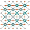
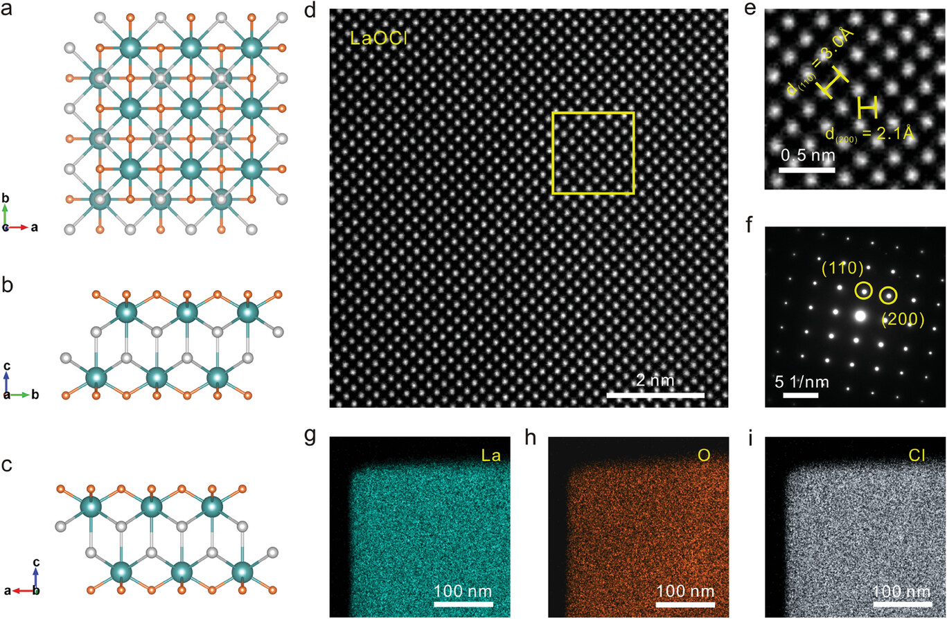
Atomic construction of ultrathin vdW LaOCl single crystals. a−c) Crystal construction of ultrathin LaOCl nanosheet alongside the c-axis, a-axis, and b-axis. d−f) HAADF-STEM, and SAED of an ultrathin vdW LaOCl single crystal. The magnified STEM picture in (e) is from the yellow field area in (d). g−i) EDS elemental mapping of an ultrathin vdW LaOCl nanosheet. (Reprinted with permission by Wiley-VCH Verlag)
The most typical gate dielectric is silicon dioxide, identified usually as glass, owing to its amorphous construction. Although considerable and readily deposited, SiO2 includes a modest dielectric fixed, limiting its final thinness and subsequently the channel size of transistors it will probably isolate.
Extra lately, the trade has adopted hafnium-based isolators like HfO2 to permit for smaller gates. Nevertheless, their innate structural dysfunction offers rise to dangling bonds, trapped expenses, and floor roughness that degrade system efficiency and reliability.
2D supplies have gained consideration for his or her potential to proceed historic scaling tendencies as soon as silicon nears its bodily limits. Their layered crystalline construction lacks out-of-plane dangling bonds and may conform intimately with adjoining strata.
Nevertheless, figuring out an appropriate insulator that bonds nicely to semiconductors like MoS2 with out ruining their pristine digital properties has remained an unsolved quandary. Researchers have solely achieved high-performing prototypes by counting on polymer separators which can’t survive manufacturing environments or match the consistency of conventional oxide movies.
Lanthanum oxychloride distinguishes itself with a large bandgap exceeding 4 eV and towering dielectric fixed over 10, translating to wonderful insulating functionality in nanometer-thin sheets.
For comparability, workhorse silicon dioxide has a modest dielectric fixed round 4, whereas higher-performance hafnia movies nonetheless prime out below 30. The sizable discrepancy straight permits lanthanum oxychloride layers to raised focus electrical fields utilizing much less materials. And even minute present leakage by means of an ultrahigh-Ok gate stack might corrupt built-in logic or reminiscence. Lanthanum oxychloride’s considerably widened bandgap consequently blocks extra tunneling electrons.
Moreover, The anisotropic crystals additionally inherently terminate with full LaCl3 layers, rendering dangling bond-free surfaces. Dangling bonds are incomplete molecular connections that degrade materials efficiency and reliability. Along with the fabric’s easy exfoliation and stacking, these traits hinted at supreme integration with 2D channel supplies, spurring investigation into synthesis methods.
Along with the fabric’s easy exfoliation and stacking, these traits hinted at supreme integration with 2D channel supplies, spurring investigation into synthesis methods.
The researchers’ customized low-pressure vapor deposition process utilizing LaCl3 and La2O3 precursors permits precision management over lanthanum oxychloride nucleation and progress kinetics. Regulating the deposited movie’s thickness, they produced samples as skinny as 1.3 nm, comprising simply two molecular layers.
Subsequent atomic pressure and transmission electron microscopy verified a pristine, extremely ordered construction nearly fully devoid of defects. X-ray photoelectron spectroscopy and diffraction affirm the right elemental composition and bonding throughout the materials.
To characterize the dielectric properties experimentally, the staff first constructed metal-insulator-metal capacitor constructions that includes lanthanum oxychloride. Electrical probing returned an distinctive dielectric fixed of 10.8 together with excellent insulating efficiency quantified by miniscule leakage present. This low conductivity trounces typical figures for each standard silicon dioxide and former best-in-class experimental dielectrics like boron nitride. Measuring extraordinarily excessive breakdown area strengths exceeding 10 MV/cm additional proves the viability for nanoelectronics purposes demanding ultrathin, flawless movies.
Integrating their vapor-grown crystals as top-gate dielectrics onto exfoliated molybdenum disulfide yielded transistors switching on and off over 4 orders of magnitude, aggressive with state-of-the-art demonstrations however counting on a deposition-compatible insulator stack.
Low hysteresis values down to just about zero noticed upon sweeping gate voltage verifies suppression of cost trapping typically plaguing units with imperfect interfaces. Hysteresis refers to variation within the digital state or output worth relying on whether or not voltage is ramped up or down. Negligible variation between from side to side traits signifies stability amenable to digital logic.
Negligible variation between from side to side traits signifies stability amenable to digital logic. Simulation and spectroscopy outcomes affirm a large bandgap MoS2 layer electronically remoted from the overlaying interconnects and substrate influences that may intervene with transport.
The researchers attribute such wonderful performance to sturdy van der Waals bonding between the layered supplies, producing an atomically sharp junction with out dysfunction.
Ongoing transistor scaling has enabled exponential computing efficiency positive factors for many years in accordance with Moore’s Legislation projections. Whereas silicon nonetheless has legs within the close to future due to novel architectures, supplies like two-dimensional semiconductors and atomically flat dielectrics will develop into important for development inside this decade.
Demonstrating the immense promise of lanthanum oxychloride movies with properties superior to standard insulators, this analysis opens the door to next-generation electronics counting on layered van der Waals stacking.
Compatibility with current foundry processes and environments gives a path for fast manufacturing scale-up. By addressing earlier roadblocks, the depressingly elusive aim of quicker, smaller, cheaper computing now appears achievable by means of hybrid materials integration.
Get our Nanotechnology Highlight updates to your inbox!
Thanks!
You might have efficiently joined our subscriber record.
Grow to be a Highlight visitor writer! Be part of our giant and rising group of visitor contributors. Have you ever simply printed a scientific paper or produce other thrilling developments to share with the nanotechnology neighborhood? Right here is learn how to publish on nanowerk.com.


